The basic premise of electronic imaging is that light energy is converted into electricity in a way that preserves visual information, allowing us to reconstruct the optical properties of a scene. This predictable interaction between photons and electrons initiates the process of capturing digital images. After the energy delivered by incident photons is converted into electrical energy, the system must have some way to quantify this energy and store it as a sequence (or matrix) of values.
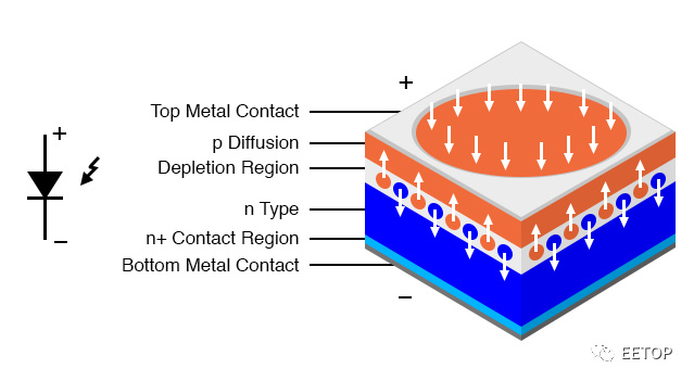
In most image sensors, the conversion from light to electricity is done by a photodiode, which is a PN junction whose structure favors the generation of electron-hole pairs in response to incident light.

Photodiodes are usually made of silicon, but other semiconductor materials such as indium arsenide, indium antimonide, mercury cadmium telluride, etc. are also used for various special purposes.
An important advance in image sensor technology was the creation of a pinned-type photodiode. In the image above, a photodiode, like a normal diode, consists of a p-type region and an n-type region.
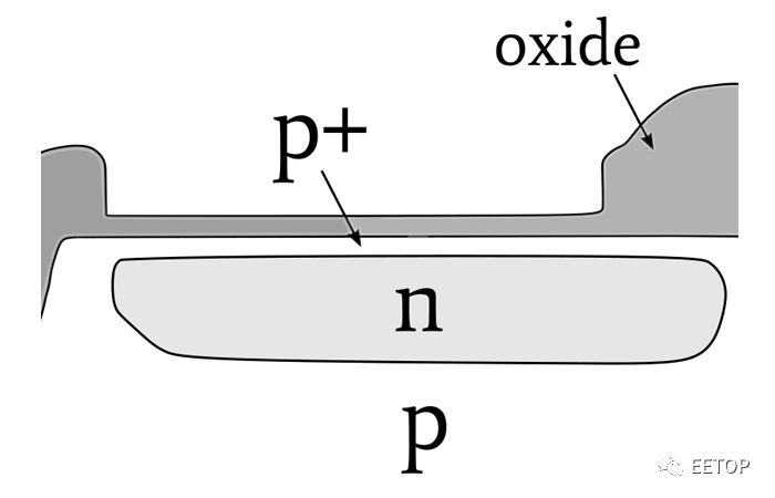
Pinned-type photodiodes have an additional region made of highly doped p-type (p+ for short) semiconductor; as shown, it is thinner than the other two regions.

This figure shows the structure of a pinned photodiode integrated into an image sensor
Introduced in the 1980s, Pinned photodiodes solved the problem (called "hysteresis") associated with the delayed transfer of light-generated charge. Pinned-style photodiodes also offer higher quantum efficiency, improved noise performance, and lower dark current (we'll return to these concepts later in this series).
Today, the photosensitive element in almost all CCD and CMOS image sensors is a Pinned photodiode.
The two main imaging technologies are CCD (Charge Coupled Device) and CMOS.
There are also other types of sensors, such as NMOS sensors for spectroscopy, miniature photometers providing infrared thermal imaging sensitivity, and special applications may use photodiode arrays connected to custom amplifier circuits.
Nonetheless, we will focus on CCD and CMOS. These two general sensor categories cover a very wide range of applications and functions.
It seems that people are drawn to the value judgment of "Which is better?" Questions like surface mount or through-hole? BJT or FET? Canon or Nikon? Windows or Mac (or Linux)? These questions rarely have meaningful answers, and even comparing individual features can be difficult.
So, which is better, CMOS or CCD? The traditional comparison goes like this: CCD has lower noise, better pixel-to-pixel uniformity, and has a reputation for superior image quality. CMOS sensors offer higher levels of integration - reducing complexity for circuit designers - and lower power consumption.
I'm not saying this assessment is inaccurate, but its usefulness is limited. A lot depends on your needs for sensors and your requirements and priorities.
In addition, technology is changing rapidly, and the large amount of money invested in digital imaging research and development may gradually change the pattern of CCD and CMOS.
Second, image sensors do not produce images. It is an integral part of a digital imaging system (a very important part, of course), and the perceived image quality produced by the system depends not only on the sensor, but many more factors. There is no doubt that CCDs outperform CMOS sensors for some optoelectronic properties. But associating a CCD with higher overall image quality seems a bit unreasonable.
System Design Considerations
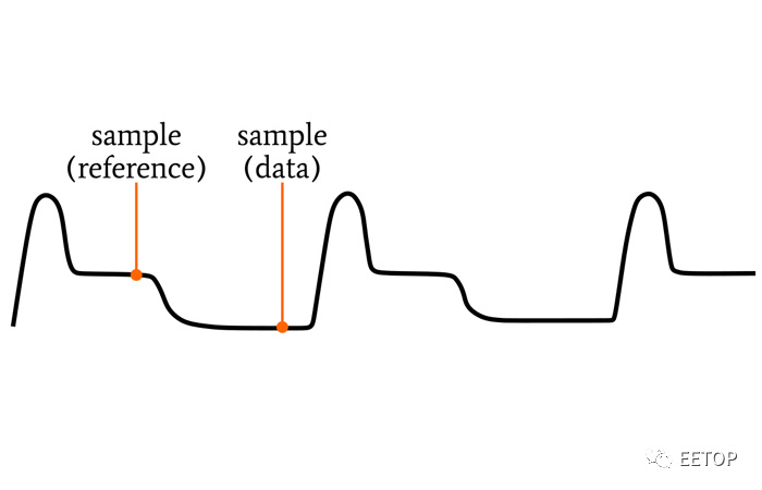
A CCD sensor-based system requires a large design investment. CCDs require a variety of non-logic-level power and control voltages (including negative voltages), and the timing that must be applied to the sensor can be very complex. The image "data" produced by the sensor is an analog waveform that needs to be finely amplified and sampled, and of course any signal processing or data conversion circuitry has the potential to introduce noise.
Low noise performance starts with a CCD, but it doesn't end there - we must strive to minimize noise throughout the signal chain.

CCD output waveform
The situation is quite different for CMOS image sensors. They work more like standard integrated circuits, with logic-level voltage sources, on-chip image processing, and digital output data. You may also have to deal with some additional image noise, but in many applications this is a small price to pay for greatly reducing design complexity, development cost and stress.
Image processing is not a typical microcontroller task, especially when you are working with high frame rate or high resolution sensors. Most applications will benefit from the computing power of a digital signal processor or FPGA.
Compression also needs to be considered, especially if you need to store images in memory or transfer them wirelessly. This can be performed by software or programmable hardware.
 English
 日本語
日本語 한국어
한국어 français
 Deutsch
 Español
 italiano
 русский
 português
 العربية
 tiếng việt
 ไทย
ไทย čeština
 dansk
dansk Svenska
